
资料下载


2.5V至5.5V400μ四电压输出8/10/12位DAC采用16引脚TSSOP封装ad5307/ad5317/ad5327数据表
分享资料个
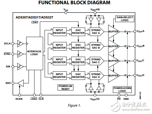
The AD5307/AD5317/AD53271 are quad 8-,10-,12-bit buffered voltage-output DACs in 16-lead TSSOP that operate from single 2.5 V to 5.5 V supplies and consume 400 μA at 3 V. Their onchip output amplifiers allow the outputs to swing rail-to-rail with a slew rate of 0.7 V/μs. The AD5307/AD5317/AD5327 utilize versatile 3-wire serial interfaces that operate at clock rates up to 30 MHz; these parts are compatible with standard SPI, QSPI, MICROWIRE, and DSP interface standards. The references for the four DACs are derived from two reference pins (one per DAC pair)。 These reference inputs can be configured as buffered or unbuffered inputs. Each part incorporates a poweron reset circuit, ensuring that the DAC outputs power up to 0 V and remain there until a valid write to the device takes place. There is also an asynchronous active low CLR pin that clears all DACs to 0 V. The outputs of all DACs can be updated simultaneously using the asynchronous LDAC input. Each part contains a power-down feature that reduces the current consumption of the device to 300 nA @ 5 V (90 nA @ 3 V)。 The parts can also be used in daisy-chaining applications using the SDO pin. All three parts are offered in the same pinout, allowing users to select the amount of resolution appropriate for their application without redesigning their circuit board.
声明:本文内容及配图由入驻作者撰写或者入驻合作网站授权转载。文章观点仅代表作者本人,不代表电子发烧友网立场。文章及其配图仅供工程师学习之用,如有内容侵权或者其他违规问题,请联系本站处理。 举报投诉
- 相关下载
- 相关文章


