
资料下载


单片16位数模转换器端口ad669数据表
分享资料个
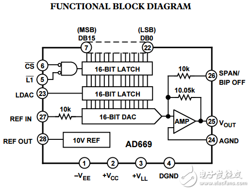
The AD669 DACPORT® is a complete 16-bit monolithic D/A converter with an on-board reference and output amplifier. It is manufactured on Analog Devices’ BiMOS II process. This process allows the fabrication of low power CMOS logic functions on the same chip as high precision bipolar linear circuitry. The AD669 chip includes current switches, decoding logic, an output amplifier, a buried Zener reference and double-buffered latches. The AD669’s architecture insures 15-bit monotonicity over temperature. Integral nonlinearity is maintained at ±0.003%, while differential nonlinearity is ±0.003% max. The on-chip output amplifier provides a voltage output settling time of 10 µs to within 1/2 LSB for a full-scale step. Data is loaded into the AD669 in a parallel 16-bit format. The double-buffered latch structure eliminates data skew errors and provides for simultaneous updating of DACs in a multi-DAC system. Three TTL/LSTTL/5 V CMOS compatible signals control the latches: CS, L1 and LDAC. The output range of the AD669 is pin programmable and can be set to provide a unipolar output range of 0 V to +10 V or a bipolar output range of –10 V to +10 V. The AD669 is available in seven grades: AN and BN versions are specified from –40°C to +85°C and are packaged in a 28-pin plastic DIP. The AR and BR versions are specified for –40°C to +85°C operation and are packaged in a 28-pin SOIC. The SQ version is specified from –55°C to +125°C and is packaged in a hermetic 28-pin cerdip package. The AD669 is also available compliant to MIL-STD-883. Refer to the AD669/883B data sheet for specifications and test conditions.
声明:本文内容及配图由入驻作者撰写或者入驻合作网站授权转载。文章观点仅代表作者本人,不代表电子发烧友网立场。文章及其配图仅供工程师学习之用,如有内容侵权或者其他违规问题,请联系本站处理。 举报投诉
- 相关下载
- 相关文章


