
资料下载


8-Lead LLP Thermal Performance a
951414
分享资料个
The new leadless leadframe package (LLP) provides significantly increased power dissipation capability in a tiny surface-mount package. The key feature of the LLP is that it has a center metal area located directly below the die which allows a direct path for heat to flow out, providing very low thermal resistance. When this pad is connected to PC board copper to provide heatsinking, values of total thermal resistance (junction-to-ambient) below 40˚C/W can be obtained in still air environments.

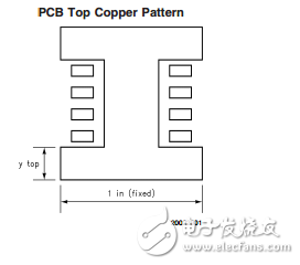
Modelling Assumptions The data listed in this application note is derived from finite element modelling in which the following assumptions are used: 1. DAP (die attach paddle) size = 3.0 mm x 2.2 mm 2. Die size = 2.11 mm x 1.63 mm 3. Package size = 4.0 mm x 4.0 mm x 0.75 mm 4. Power Dissipation = 1W 5. Thermal Vias (0.3 mm diameter) = 8 Copper Patterns Data is provided for PCB designs using copper patterns which are ’dog-bone’ shaped on the top layer and a square pattern directly beneath the part on the bottom layer (see below). In the bottom layer pattern, the X and Y dimensions are equal. P
声明:本文内容及配图由入驻作者撰写或者入驻合作网站授权转载。文章观点仅代表作者本人,不代表电子发烧友网立场。文章及其配图仅供工程师学习之用,如有内容侵权或者其他违规问题,请联系本站处理。 举报投诉
- 相关下载
- 相关文章


