资料下载

两个可选的输入低电压输出硅锗时钟分列缓冲器adclk948数据表
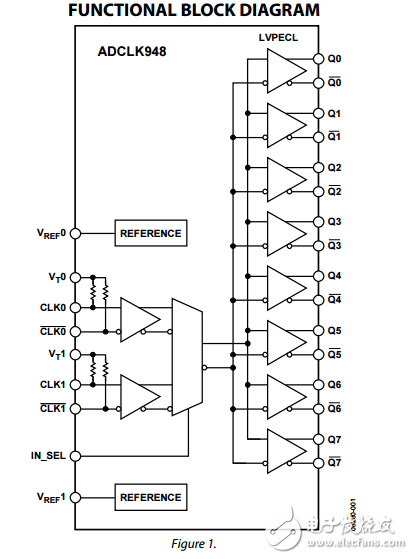
The ADCLK948 is an ultrafast clock fanout buffer fabricated on the Analog Devices, Inc., proprietary XFCB3 silicon germanium (SiGe) bipolar process. This device is designed for high speed applications requiring low jitter. The device has two selectable differential inputs via the IN_SEL control pin. Both inputs are equipped with center tapped, differential, 100 Ω on-chip termination resistors. The inputs accept dc-coupled LVPECL, CML, 3.3 V CMOS (single-ended), and ac-coupled 1.8 V CMOS, LVDS, and LVPECL inputs. A VREFx pin is available for biasing ac-coupled inputs. The ADCLK948 features eight full-swing emitter coupled logic (ECL) output drivers. For LVPECL (positive ECL) operation, bias VCC to the positive supply and VEE to ground. For ECL operation, bias VCC to ground and VEE to the negative supply. The output stages are designed to directly drive 800 mV each side into 50 Ω terminated to VCC − 2 V for a total differential output swing of 1.6 V. The ADCLK948 is available in a 32-lead LFCSP and specified for operation over the standard industrial temperature range of −40°C to +85°C.

声明:本文内容及配图由入驻作者撰写或者入驻合作网站授权转载。文章观点仅代表作者本人,不代表电子发烧友网立场。文章及其配图仅供工程师学习之用,如有内容侵权或者其他违规问题,请联系本站处理。 举报投诉
- 相关下载
- 相关文章


