
资料下载


可编程低电压1:10 LVDS时钟驱动器adn4670数据表
分享资料个
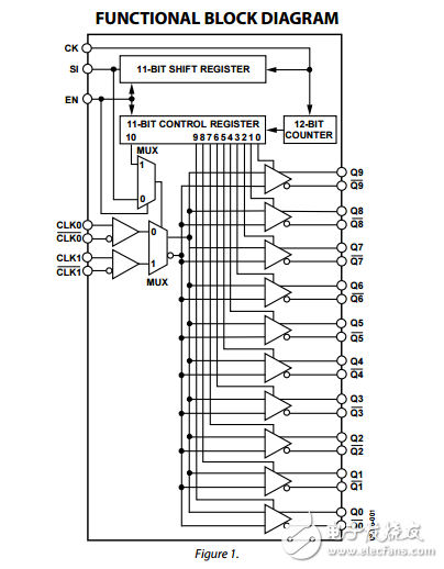
The ADN4670 is a low voltage differential signaling (LVDS) clock driver that expands a differential clock input signal to 10 differential clock outputs. The device is programmable using a simple serial interface, so that one of two clock inputs can be selected (CLK0/CLK0 or CLK1/CLK1) and any of the differential outputs (Q0/Q0 to Q9/Q9) can be enabled or disabled (tristated)。 The ADN4670 is designed for use in 50 Ω transmission line environments. When the enable input EN is high, the device may be programmed by clocking 11 data bits into the shift register. The first 10 bits determine which outputs are enabled (0 = disabled, 1 = enabled), while the 11th bit selects the clock input (0 = CLK0, 1 = CLK1)。 A 12th clock pulse transfers data from the shift register to the control register. The ADN4670 is fully specified over the industrial temperature range and is available in a 32-lead LFCSP and LQFP packages.
声明:本文内容及配图由入驻作者撰写或者入驻合作网站授权转载。文章观点仅代表作者本人,不代表电子发烧友网立场。文章及其配图仅供工程师学习之用,如有内容侵权或者其他违规问题,请联系本站处理。 举报投诉
- 相关下载
- 相关文章


